
PCBA Manufacturing Process Technology
This article explains practical PCBA manufacturing technology from incoming-material checks through final testing on a standard SMT/assembly line. It focuses on measurable, repeatable floor-level controls that directly affect solder quality, placement accuracy, reflow stability, inspection predictability and reproducible diagnostics used by engineers and technicians on real production floors. The goal is to outline methods that work on factory equipment—not lab-only instrumentation.
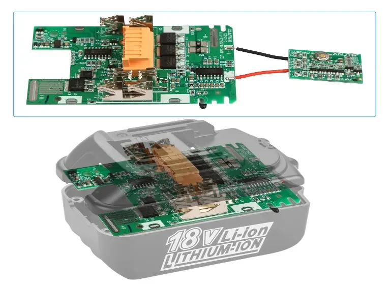
What is PCBA?
A PCBA (Printed Circuit Board Assembly) is the completed electronic module after components such as ICs, resistors, capacitors, MOSFETs, sensors, and connectors are mounted onto a bare PCB using SMT and/or THT processes. A PCBA includes solder joints, firmware-loaded devices, inspection/test data, and electrical performance characteristics, and it serves as the functional core of chargers, BMS boards, tools, appliances, and industrial equipment.
Why Is Safety the First Constraint in Any PCBA Manufacturing Line?
Safety begins with strict ESD controls: grounded benches, continuous wrist-strap monitors, ionizers positioned at the print station and high-density feeder areas, and humidity kept within the 45–60% range to reduce static events. Hot processes—reflow ovens, wave/selective solder, preheaters—and chemical materials such as no-clean fluxes, IPA, and solder-paste solvents must be handled under MSDS instructions with PPE and exhaust ventilation. Only trained technicians should energize boards, especially high-current assemblies, and any sign of smoke, electrolyte odor, abnormal heating or sudden inrush current must trigger immediate line stop and lot quarantine. These safeguards ensure that process control can proceed without safety-induced variability.
Transition: With safety secured, the next step is understanding how a complete SMT workflow is executed in real factories.
How Does a Real SMT/Assembly Line Execute the PCBA Manufacturing Workflow?
-
Incoming material check:
Inspect PCB solderability, warpage (<0.75%), surface finish condition (ENIG/OSP integrity), moisture level per IPC-1601, and MSL bag integrity for ICs. Verify component reel traceability, date codes and storage conditions. Measure solder-paste temperature and confirm lot/expiry before loading. -
Stencil & printing:
Ensure stencil flatness, aperture wall cleanliness and correct tension. Validate alignment using fiducials. Adjust print pressure, speed, separation, and stencil wipe interval based on early SPI data. Stable paste transfer rates (>80%) are targeted. -
Paste handling:
Allow controlled warm-up to prevent condensation. Monitor viscosity shifts with SPI volume trends or manual slump checks. Enforce fixed open-time and shelf-life windows on the printer to avoid drying, oxidation or separation. -
Pick-and-place:
Verify feeder loading, tape peel force, nozzle condition and reference-point calibration. Use first-article inspection for rotation, polarity, and fine-pitch alignment. Track mis-pick rates and feeder drift to prevent repetitive placement faults. -
Reflow soldering:
Use thermocouple profiling to measure ramp rate, soak temperature, TAL (time above liquidus) and peak temperature. Re-profile whenever PCB thickness, copper stackup, or BGA density changes. Monitor joint fillet shape, voiding and grain structure trends for long-term reliability. -
Secondary/through-hole ops:
Control wave/selective-solder parameters such as preheat delta-T, nozzle angle, solder depth and flux deposition. For mixed-technology products, enforce strict order: SMT → reflow → THT → cleaning → conformal coat if required. -
AOI / X-ray:
AOI parameters must match the board’s component library for accurate lead, polarity and fillet interpretation. X-ray is used for BGAs, LGA/QFN thermal pads and high-density power stages to detect voids, opens and head-in-pillow defects. -
Electrical test & programming:
Check inrush current, quiescent current, power-good timing, logic boot and major functional nodes. Program firmware using guarded connectors with ESD-safe fixtures. Validate hardware–firmware compatibility per lot. -
Line-level reliability screens:
Apply light cyclic loading, short thermal exposure and mechanical agitation to reveal marginal solder joints, connector issues or insufficient wetting. -
Final check & packing:
Confirm label correctness, serialization, QR/UID readability and anti-static protective packaging to avoid board flex or moisture absorption during shipment.
Transition: With the workflow clear, the next step is identifying the technology decisions that most influence reliability.
Which Key Technology Decisions Have the Greatest Impact on PCBA Reliability?
Reliability is shaped early through decisions on stencil aperture reductions, solder-paste formulation (SAC305 vs. low-voiding blends), flux activation level, component package size, pad design, copper distribution and the required reflow profile. These choices determine wetting balance, intermetallic compound (IMC) growth rate, void level, fillet geometry and long-term fatigue resistance. For BGA assemblies, paste-volume symmetry and thermal uniformity are the highest-impact contributors to stable yield.
Transition: Technology alone cannot maintain stability—floor-level reproducible controls make or break real production.
What Reproducible, Floor-Friendly Methods Keep SMT Processes Stable?
How Do You Verify SMT Print Quality?
Perform visual checks on the first two to five panels. Run SPI with volume, height and area thresholds aligned to IPC-7525 guidelines. If transfer efficiency drops, inspect stencil aperture walls and verify squeegee flatness and pressure uniformity. Clean stencil on a fixed cycle rather than reactive cleaning to maintain output consistency.
How Do You Confirm Pick-and-Place Accuracy?
Use microscope or vision-aligned first-article checks. Verify component offset (<25% of pad width), rotation (<2°) and polarity on sensitive ICs. Track mis-picks per feeder per hour. Clean nozzles and recalibrate feeders when repeated positional drift or pickup failures are seen.
How Do You Maintain Reflow Stability?
Re-profile at the start of each shift or whenever board density changes. Confirm peak temperature within ±3 °C of target and maintain ramp rate below 3 °C/s to limit tombstoning. Monitor cooling gradients to prevent thermal shock and grain coarsening.
How Do You Validate AOI/X-ray Outputs?
Optimize AOI recipes per board family, reducing false calls while maintaining coverage. Use X-ray image libraries of known-good samples to anchor defect judgment. Track trends in BGA voiding, HIP defects or bridging to detect reflow drift before major failures occur.
How Do You Verify Core Electrical Function?
Define baseline boot time, quiescent current windows, voltage rail sequencing and I/O behavior. Compare electrical failures with corresponding AOI/X-ray signatures to shorten corrective-action cycles.
Transition: With inspections stable, the next layer is lightweight reliability screening.
Which Practical Reliability Screens Can Be Run Directly on the Production Line?
Apply:
• Moderate power cycling: Reveals cold joints, marginal MOSFET gates or unstable converters.
• Short thermal soak (40–50 °C): Detects thermally sensitive cracks or insufficient solder wetting.
• Vibration/tap tests: Identifies weak connector pins, insufficient THT fill or brittle joints.
• Humidity-wipe checks: Highlights flux reactivity and improper cleaning in coated or high-voltage boards.
These “quick screens” require minimal equipment and expose borderline assemblies before they escape the factory.
Transition: Reliability screens highlight failure patterns—the next step is fast diagnosis.
What Are the Most Common SMT/Assembly Defects and How Do You Fix Them?
-
Solder bridging: Caused by excess paste volume, poor stencil release or misalignment → adjust apertures (reduce 5–10%), clean stencil, refine separation speed.
-
Tombstoning: Imbalanced paste volumes or aggressive thermal ramp → modify aperture reduction ratio, slow initial ramp.
-
Insufficient solder: Due to paste oxidation, low deposit or inadequate peak temp → verify paste age, increase print volume, adjust TAL.
-
BGA voiding: Often from moisture or aggressive ramp → pre-bake PCBs, add soak stage, use low-void paste.
-
Wrong component/misfeed: Feeder drift or operator error → enforce barcode verification, retrain setup, maintain peel-force stability.
-
Post-rework failure: Excessive heating or pad lift → use rework profiles, inspect pads before reflow.
Transition: Once defects are identified, quick triage keeps the line moving.
How Do You Troubleshoot PCBA Problems and Perform Fast Field Triage?
-
Categorize symptoms: loss of function, unstable current, thermal rise, intermittent failure.
-
Trace back through the process chain: print → place → reflow → secondary → test/program.
-
Compare multiple failing units for recurring patterns.
-
Apply targeted fixes: adjust stencil cleaning, re-tune reflow, clean nozzles, correct feeder alignment or replace components.
-
Re-run production tests before re-releasing the lot.
Transition: Maintaining quality requires ongoing data-driven refinement.
How Do Engineering Teams Maintain Continuous Improvement in PCBA Lines?
Use SPI/AOI statistical data to refine stencil apertures and placement offsets. Update reflow profiles when material stacks change. Maintain golden boards for electrical and visual reference. Trend defect logs weekly to plan maintenance cycles for stencils, feeders and oven zones. Conduct first-article reviews per shift to catch early drift.
FAQ
1. Why is solder paste control critical in PCBA?
Paste volume directly affects joint strength, wetting quality, and the probability of defects like bridging, head-in-pillow, voiding, and open circuits. Stable viscosity and accurate stencil parameters are essential.
2. What causes component tombstoning?
Imbalanced solder wetting forces during reflow, uneven pad design, temperature gradients, or excessive paste volume on one side can lift small passive components vertically.
3. Why do some boards require X-ray inspection?
X-ray is necessary when components have hidden joints (BGA, QFN, power packages, bottom-terminated devices) because AOI cannot detect the quality of solder underneath the package.
4. What is the purpose of ICT vs. FCT?
ICT verifies component values, shorts, opens, and net integrity. FCT validates real electrical behavior under operating conditions—voltage, current, signals, and firmware functionality.
5. Why does reflow temperature need profiling?
Each board has unique thermal mass and requires a controlled soak/reflow curve to ensure proper wetting without overheating components. Deviation can cause cold joints, burnt flux, or cracked packages.
6. What factors most affect SMT placement accuracy?
Feeder calibration, nozzle condition, vision alignment, component packaging quality, and stable PCB support. Warped boards or unstable vacuum pickup also reduce accuracy.
7. Why do some PCBAs fail only after assembly into a product?
Mechanical stress, enclosure heat trapping, screw torque deformation, connector strain, or vibration may expose marginal solder joints or borderline components that passed initial tests.
8. How does conformal coating affect PCBA reliability?
Coating protects against moisture, dust, ionic contamination, and corrosion. However, poor masking or uneven coating can trap flux residue, causing long-term leakage paths.
9. What are common thermal issues on high-current PCBAs?
Hotspots around MOSFETs, shunts, inductors, or power ICs; insufficient copper area; inadequate vias; or poor airflow. These increase resistance and reduce long-term reliability.
10. Why is component traceability needed?
It allows engineers to link failures to specific batches, reflow lots, or material changes, enabling faster root-cause identification for field returns.
11. What does a good PCBA test report typically include?
Electrical measurements, functional pass/fail records, firmware version, reflow data, serial/QR information, and any thermal or stress-test observations. (No procurement or acceptance requirements involved.)
Conclusion — What Ultimately Ensures Stable, Reliable PCBA Output?
Stable PCBA production relies on controlled printing, accurate placement, consistent reflow and disciplined electrical testing. Using measurable first-article checks, actionable inspection data and closed-loop improvement creates predictable yield without requiring lab-level equipment. Consistency—not complexity—is the foundation of long-term reliability in SMT manufacturing.