
Tool Battery BMS Miniaturization: Protection IC & MOSFET Trends
Shrinking protection ICs and more compact MOSFET power-paths are reshaping modern tool-battery BMS architecture. This brief explains the engineering tradeoffs (thermal, EMI, reliability, manufacturability), how to test and validate miniaturized designs, and what procurement and maintenance teams must require from vendors.
Miniaturization raises power density, thermal concentration, and handling risk. Any pack that smokes, swells, emits odor, or overheats must be isolated outdoors on a non-combustible surface, labeled QUARANTINE, and handled via disposal/RMA procedures. Board-level work requires ESD controls, proper isolation, and qualified technicians. Never probe high-current live paths without current limiting.
2 · What “miniaturization” means for BMS and power-path design
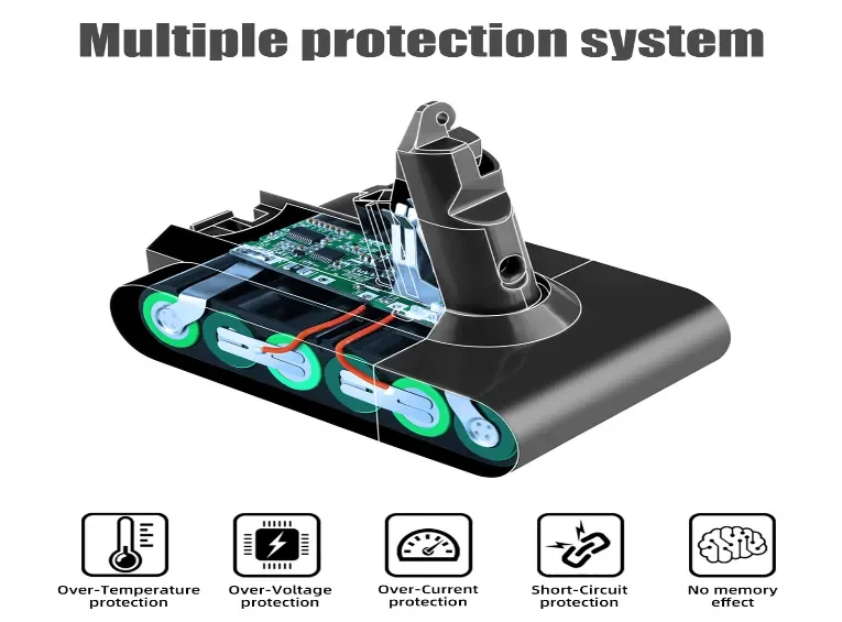
Miniaturization covers smaller protection ICs (monitor + balance + driver in one), compact MOSFET packages with lower Rds(on), integrated gate drivers, embedded current sensing, smart power-path controllers, and denser PCB layouts. Benefits: smaller PCB footprint, lower part counts, and potentially lower cost. Tradeoffs: tighter thermal budgets, higher EMI sensitivity, reduced repairability, and stricter manufacturing tolerances.
3 · Key technical trends driving miniaturized BMS designs
-
Highly integrated protection ICs combining monitoring, balancing, and gate driving.
-
Integrated dual-FET packages and MOSFET arrays concentrating thermal load.
-
Lower Rds(on) from silicon advances and refined leadframe/copper designs.
-
Shift to SMD power packages (Power QFN, LFPAK, eSOP) requiring optimized via stitching and reflow profiles.
-
Embedded current sensing (on-chip ADCs, integrated Hall) needing accurate calibration.
-
Smart power-path controllers replacing discrete MOSFET drivers.
-
Limited use of GaN/SiC in front-end or fast-charge stages.
-
Firmware-driven SOA protections, thermal derating curves and adaptive error logic.
-
Increased EMI susceptibility from short switching loops and compact layouts.
-
Long-term reliability concerns (solder fatigue, vibration, mechanical stress).
4 · Design implications engineers must address
-
Thermal strategy: copper pours, thermal vias, heatspreaders; validate θJA experimentally.
-
Minimize high-current loop area to lower switching losses and EMI.
-
EMI mitigation: ferrite beads, common-mode chokes, controlled ground strategy, and careful return routing.
-
Accurate current-sense layout and calibration to prevent offset or drift.
-
Firmware enforcement of SOA limits, derating tables and robust fault logic.
-
Mechanical reinforcement: vibration-resistant soldering, glue, or retention features for stressed zones.
-
Maintain test pads and debug hooks for manufacturing visibility and field diagnostics.
5 · Acceptance and test protocol for miniaturized BMS hardware
A. Bench electrical tests
-
Measure Rds(on) at 25 °C and elevated temperatures.
-
High-current pulse tests (1–2× rated peak) while logging ΔT and gate voltage.
-
Short-circuit and overcurrent protection timing verification.
-
Integrated driver timing and controller response checks.
B. Thermal & mechanical tests
-
IR thermal mapping under realistic duty cycles and worst-case scenarios.
-
Vibration and thermal cycling per vendor spec or MIL-STD where applicable.
-
X-ray or optical inspection of solder joints and package integrity.
C. EMI & signal-integrity tests
-
Radiated and conducted EMI scans in the assembled enclosure.
-
Verify tool↔pack and charger↔pack comms remain reliable under EMI stress.
D. Field pilot
-
30–90 day pilot logging peak currents, thermal derates, transient faults and resets.
-
Acceptance criteria: meet ΔT limits, fault-rate thresholds and cross-sample consistency.
6 · Starting acceptance thresholds for procurement and engineering
-
ΔRds(on) drift after 1,000 pulses: < 10%.
-
Maximum component temperature: ≤ 85 °C (or vendor-specific rating).
-
Thermal hotspot: no area > ambient + 40 °C under defined duty.
-
Overcurrent cutoff response: within vendor-specified millisecond window.
-
EMI compliance: emissions must pass applicable CE/FCC limits and not disrupt comms.
Adjust thresholds per application, chemistry, and use profile.
7 · Procurement language that protects buyers
Supplier shall disclose full BOM (protection IC and MOSFET PNs), θJA/thermal resistance data, pack-level thermal maps under defined duty profiles, high-current pulse logs, and provide pilot units for a 90-day field evaluation. Warranty must cover thermal and board-level failures for 12 months. Vendor must support RMA and root-cause data for units exceeding acceptance thresholds. Production lots must include accessible test pads and one golden reference unit.
Require signed test reports and raw logs as part of acceptance.
8 · Maintenance & service best practices for miniaturized assemblies
-
Perform periodic IR scans to monitor hotspot drift.
-
Archive BMS event counters, derate logs and fault traces for RMA investigations.
-
Prefer module replacement over field rework due to fragile solder joints.
-
Require thermal images and raw logs from vendors for all returns.
9 · Risks introduced by miniaturized power-path hardware
| Risk | Likelihood | Impact | Primary mitigations |
|---|---|---|---|
| Thermal concentration in compact FETs | High | High | Copper pours, vias, IR validation |
| EMI disrupting communications | Medium | Medium | Filtering, grounding, layout rules |
| Solder fatigue under vibration | Medium | High | Reinforced joints, vibration testing |
| Inaccurate current sensing | Medium | Medium | Guard traces, calibration procedures |
Track these systematically during pilot and production ramp.
10 · Common qualification questions
Q: Do smaller MOSFET packages always reduce losses?
A: Not necessarily—thermal resistance can increase. Measure ΔV, ΔT and θJA rather than assuming lower Rds(on) equals lower system loss.
Q: Are highly integrated protection ICs acceptable?
A: Yes if vendors supply thermal maps, SOA margins, and pilot test evidence covering edge cases.
Q: Is GaN realistic inside handheld packs?
A: Rare for discharge FETs today; more relevant for chargers or specialty fast-charge front ends.
11 · Final takeaway
Miniaturized protection ICs and MOSFETs deliver smaller footprints and reduced BOM complexity but shift failure modes into thermal, EMI, and mechanical domains. Validate through pulse, thermal, EMI testing and a structured field pilot before scaling production. Require vendor transparency—part numbers, thermal data, raw logs—and insist on accessible test points on production units.